Schemes of regulated power supplies on the kr142en22a chip. DIY universal power supply
A lot of amateur radio power supplies (PSUs) are made on KR142EN12, KR142EN22A, KR142EN24 chips, etc. The lower adjustment limit of these microcircuits is 1.2 ... 1.3 V, but sometimes a voltage of 0.5 ... 1 V is necessary. The author offers several technical solutions for a power supply unit based on these microcircuits.
The integrated circuit (IC) KR142EN12A (Fig. 1) is an adjustable voltage regulator of the compensation type in the KT-28-2 package, which allows you to power devices with a current of up to 1.5 A in the voltage range of 1.2 ... 37 V. This integrated The stabilizer has thermally stable current protection and output short circuit protection.
Fig.1. IC KR142EN12A
Based on the IC KR142EN12A, it is possible to build an adjustable power supply, the circuit of which (without a transformer and a diode bridge) is shown in Fig. 2. The rectified input voltage is supplied from the diode bridge to the capacitor C1. Transistor VT2 and chip DA1 must be located on the radiator. The heat sink flange DA1 is electrically connected to pin 2, so if DA1 and the transistor VD2 are located on the same heatsink, they must be isolated from each other. In the author's version, DA1 is installed on a separate small heatsink, which is not galvanically connected to the heatsink and transistor VT2.
Fig.2. Adjustable PSU on IC KR142EN12A
The power dissipated by a chip with a heat sink must not exceed 10 watts. Resistors R3 and R5 form a voltage divider included in the measuring element of the stabilizer, and are selected according to the formula:
U out = U out min (1 + R3/R5).
A stabilized negative voltage of -5 V is supplied to the capacitor C2 and resistor R2 (used to select the thermally stable point VD1).
To protect against a short circuit of the output circuit of the stabilizer, it is enough to connect an electrolytic capacitor with a capacity of at least 10 μF in parallel with the resistor R3, and shunt the resistor R5 with a KD521A diode. The location of the parts is not critical, but for good temperature stability it is necessary to use the appropriate types of resistors. They should be located as far as possible from heat sources. The overall stability of the output voltage is made up of many factors and usually does not exceed 0.25% after warming up.
After turning on and warming up the device, the minimum output voltage of 0 V is set by the resistor Radd. Resistors R2 (Fig. 2) and resistor Radd (Fig. 3) must be multi-turn trimmers from the SP5 series.
Fig.3. Wiring diagram Radd
The current capabilities of the KR142EN12A microcircuit are limited to 1.5 A. Currently, microcircuits with similar parameters are on sale, but designed for a higher current in the load, for example, LM350 - for a current of 3 A, LM338 - for a current of 5 A. Data on these microcircuits can be found on the National Semiconductor website.
Recently, imported microcircuits from the LOW DROP series (SD, DV, LT1083/1084/1085) have appeared on sale. These microcircuits can operate at a reduced voltage between input and output (up to 1...1.3 V) and provide a stabilized voltage at the output in the range of 1.25...30 V at a load current of 7.5/5/3 A respectively. The closest domestic analogue of the KR142EN22 type in terms of parameters has a maximum stabilization current of 7.5 A.
At the maximum output current, the stabilization mode is guaranteed by the manufacturer at an input-output voltage of at least 1.5 V. The microcircuits also have built-in protection against exceeding the current in the load of an acceptable value and thermal protection against overheating of the case.
These stabilizers provide output voltage instability of 0.05%/V, output voltage instability when the output current changes from 10 mA to the maximum value no worse than 0.1%/V.
Figure 4 shows a power supply circuit for a home laboratory, which allows you to do without transistors VT1 and VT2, shown in Figure 2. Instead of the DA1 KR142EN12A chip, the KR142EN22A chip was used. This is an adjustable regulator with a low voltage drop, allowing you to get a current of up to 7.5 A in the load.
Fig.4. Adjustable PSU on IC KR142EN22A
The maximum power dissipation at the output of the stabilizer Pmax can be calculated by the formula:
P max \u003d (U in - U out) I out,
where U in is the input voltage supplied to the DA3 chip, U out is the output voltage at the load, I out is the output current of the microcircuit.
For example, the input voltage supplied to the microcircuit is U in \u003d 39 V, the output voltage at the load U out \u003d 30 V, the current at the load I out \u003d 5 A, then the maximum power dissipated by the microcircuit at the load is 45 W.
The electrolytic capacitor C7 is used to reduce the output impedance at high frequencies, and also lowers the noise voltage level and improves ripple smoothing. If this capacitor is tantalum, then its nominal capacitance must be at least 22 microfarads, if aluminum - at least 150 microfarads. If necessary, the capacitance of the capacitor C7 can be increased.
If the electrolytic capacitor C7 is located at a distance of more than 155 mm and is connected to the PSU with a wire with a cross section of less than 1 mm, then an additional electrolytic capacitor with a capacity of at least 10 microfarads is installed on the board parallel to the capacitor C7, closer to the microcircuit itself.
The capacitance of the filter capacitor C1 can be determined approximately, based on 2000 microfarads per 1 A of output current (at a voltage of at least 50 V). To reduce the temperature drift of the output voltage, the resistor R8 must be either wire or metal-foil with an error of no worse than 1%. Resistor R7 is the same type as R8. If the KS113A zener diode is not available, you can use the assembly shown in Fig. 3. The protection circuit solution given in the author is quite satisfied, as it works flawlessly and has been tested in practice. You can use any power supply protection circuitry, for example, those proposed in. In the author's version, when relay K1 is activated, contacts K1.1 close, shorting resistor R7, and the voltage at the PSU output becomes 0 V.
The printed circuit board of the power supply unit and the location of the elements are shown in Fig. 5, the appearance of the power supply unit is shown in Fig. 6. PCB dimensions 112x75 mm. Radiator selected needle. The DA3 chip is isolated from the heatsink by a gasket and attached to it with a steel spring plate that presses the chip to the heatsink.
Fig.5. PSU circuit board and element layout
Capacitor C1 of type K50-24 is composed of two capacitors connected in parallel with a capacity of 4700 μFx50 V. An imported analog of a capacitor of type K50-6 with a capacity of 10,000 μFx50 V can be used. The capacitor should be located as close as possible to the board, and the conductors connecting it to the board should be as short as possible. Capacitor C7 manufactured by Weston with a capacity of 1000 uFx50 V. Capacitor C8 is not shown in the diagram, but there are holes on the printed circuit board for it. You can use a capacitor with a rating of 0.01 ... 0.1 μF for a voltage of at least 10 ... 15 V.
Fig.6. PSU appearance
Diodes VD1-VD4 are an imported RS602 diode microassembly, designed for a maximum current of 6 A (Fig. 4). The RES10 relay (passport RS4524302) is used in the power supply protection circuit. In the author's version, a resistor R7 of the SPP-ZA type was used with a parameter spread of no more than 5%. Resistor R8 (Fig. 4) must have a spread of no more than 1% from the specified value.
The power supply usually does not require configuration and starts working immediately after assembly. After warming up the unit with resistor R6 (Fig. 4) or resistor Rdop (Fig. 3), 0 V is set at the nominal value of R7.
In this design, a power transformer of the OSM-0.1UZ brand with a power of 100 W is used. Magnetic core ShL25/40-25. The primary winding contains 734 turns of PEV wire 0.6 mm, winding II - 90 turns of PEV wire 1.6 mm, winding III - 46 turns of PEV wire 0.4 mm with a tap from the middle.
The RS602 diode assembly can be replaced with diodes rated for a current of at least 10 A, for example, KD203A, V, D or KD210 A-G (if you do not place the diodes separately, you will have to redo the printed circuit board). As a transistor VT1, you can use the transistor KT361G.
Sources
- http://www.national.com/catalog/AnalogRegulators_LinearRegulators-StandardNPN_PositiveVoltageAdjutable.html
- Morokhin L. Laboratory power supply//Radio. - 1999 - No. 2
- Nechaev I. Protection of small network power supplies from overloads//Radio. - 1996.-№12
KR142EN22A - linear adjustable voltage stabilizer of positive polarity. The case of the microcircuit is shown in Figure 2. The switching circuit of this microcircuit is shown in Figure 3.
Figure 2 Chip body

Figure 3 Typical circuit for switching on a microcircuit
Features of turning on the KR142EN22A chip:
The output voltage is calculated by the formula: Uout=1.25*(1+R1/R2)+Ireg*R2
where 1.25 V is the reference voltage (Uout), Ireg is the current in the control output circuit (100mA max);
Resistance R1 is selected in the range of 100-1000 ohms (typical 240 ohms). R2 is used to set the output voltage.
The diagram shows the minimum values of filter capacities C1 and C2 required for stable operation of the stabilizer. In practice, capacitance values range from tens to thousands of microfarads. Capacitances should be located as close as possible to the KR142EN22A chip. C1 can be combined with the rectifier filter capacitance. For larger capacities, C1>>C2 is recommended.
Capacitance Cadj is set if necessary to further reduce the output voltage ripple. Recommended Cadj< The KR142EN22A microcircuit is protected from a short-term output short circuit, but is not protected from the input short circuit - this situation, as well as any excess of the output voltage over the input voltage, leads to the failure of the microcircuit. If such a situation is possible, in particular, if the capacitance at the output of the stabilizer exceeds the capacitance at the input, a protective diode VD1 is installed. The protective diode VD2 is installed only when the capacity Cadj is installed to protect the stabilizer from discharging this capacity. The flange (radiator) of the housing of the KR142EN22A microcircuit is connected to the output terminal and therefore must be isolated from the common wire during installation. The circuit designer must understand that the maximum output current of the regulator is also limited by the maximum power dissipation of the microcircuit (in this case 30W). Iout
Pin assignment KR142EN22A
Main technical characteristics of KR142EN22A
3. Power supply with switching regulator 1.2 ... 25V
Linear stabilized power supplies have low efficiency, significant dimensions and weight. The efficiency of linear stabilized IPs (linear stabilizers) turns out to be especially low if the output voltage changes over a wide range, since a significant power is dissipated on the regulating (pass-through) transistor operating in continuous mode and being an active kind of quenching resistor. The efficiency of the stabilizers increases if the control element operates in the key (pulse) mode. At the same time, by increasing the switching frequency (up to 20 - 50 kHz instead of 50 Hz), the masses and dimensions of the transformers and capacitors of the pulsed power supply filter are significantly reduced.

Figure 4 Power supply with a switching regulator 1.2 ... 25V
A powerful laboratory power supply with a switching voltage regulator, equipped with an overload protection unit on self-restoring fuses and an audible signaling device for the presence of a short circuit or overload of its output, is considered in.
The device is assembled using the popular integrated circuit type LM2576HVT-ADJ, which is a pulsed adjustable switching DC voltage regulator. The LM2576HVT-ADJ microcircuit is capable of delivering current to the load up to 3 A. The maximum DC input voltage can be up to 63 V, the minimum output voltage is 1.2 V. The efficiency of the stabilizer at the maximum load current is about 85%. This power supply is equipped with an effective system for filtering the output voltage from noise and mains interference, which allows you to power various sound-reproducing, television and radio devices from it.
The schematic diagram of the power supply is shown in Figure 2. The output voltage of the power supply assembled according to this scheme can be adjusted from 1.2 to 25 V. The maximum allowable current of the connected load can reach 3 A over the entire range of output voltages. The output voltage ripple range does not exceed 20 mV at the maximum load current. The AC mains voltage is supplied to the primary winding of the power step-down transformer T1 through the closed contacts of the power switch SA1, fuse FU1 and resistor R2. Varistor RU1 protects the device from power surges. Resistor R2 reduces the chance of damage to the varistor. From the secondary winding of the transformer T1, an alternating current voltage reduced to 32 V is removed, which is supplied to the bridge rectifier VD1. The ripple of the rectified voltage is smoothed out by high-capacity oxide capacitors C14 and C1. Filter C13L4C18 reduces the level of mains interference, and also eliminates the possibility of penetration into the network of high-frequency interference from a working switching converter. The FU2 polymer resettable fuse protects the transformer and bridge rectifier from overload. The rectified filtered voltage is fed to the input of the DA1 integrated circuit, pin 1. The output voltage of the switching regulator is regulated by a variable resistor R6. Choke L1 - storage. The installation of two Schottky diodes VD2, VD3, connected in parallel, increases the reliability of the stabilizer when it operates at the maximum allowable load current. A three-section low-pass filter on the chokes L2, L3, L5 and their piping capacitors smooths out ripples and reduces the noise level of the output voltage. LED HL1 indicates the presence of the output voltage. The field-effect transistor VT2 works as a stable current generator, which ensures a stable brightness of the HL1 glow when the output voltage changes. Diode VD4 and resistor R5 protect the DA1 chip from damage. Resistor R14 acts as a voltage regulator load.
The output regulated stabilized voltage is supplied to the socket XS2. In order for this lithium block to be used as a laboratory one, a protection module with resettable fuses FU3 - FU5 is installed at its output. When the contacts of none of the buttons of the switch SB1 are not closed, the current flows through the weakest fuse FU5 for a rated operating current of 0.1 A. The cold resistance of this fuse is about 3 ohms. When the contacts of the SB1.1 button are closed, a self-resetting fuse FU3 is connected in parallel to it, designed for a rated operating current of 0.4 A, having a cold resistance of 0.6 Ohm. When the contacts of the button SB1.3 are closed, fuse FU4 is connected in parallel with FU5 for a current of 0.9 A with a resistance of 0.1 Ohm. With a double overload, the response time of self-restoring fuses will be about 30 s, with a fourfold overload, no more than 3 s. When the contacts of the SB1.3 button are closed, the overload protection of the load and PSU nodes is provided by the built-in protection means of the LM2576HVT-ADJ chip and the FU2 fuse. In this case, the output impedance of the PSU will be no more than 50 mΩ. Using the SB2 switch with two groups of contacts, you can completely disconnect the load from the power supply, which allows you to perform various manipulations with it with minimal risk of damaging radio components that are sensitive to static electricity and mains voltage leakage. An unstabilized voltage of about 44 V DC is supplied to the XS1 socket, it can be used to power other voltage stabilizers, UMZCH, incandescent lighting lamps for an operating voltage of 36 V with a total power of 60 ... 90 W, electric soldering irons for an operating voltage of 42 V with a power of 40 W.
On the pointer microammeter PV1, a voltmeter of the output voltage of the power supply is assembled. The VD5 zener diode is necessary for the linearization of the voltmeter scale. White LEDs HL2 - HL5 light up the scale of the voltmeter. On the MOS chip DD1, a buzzer assembly is assembled for the presence of a short circuit at the output of XS3. When there is no short circuit in the load or at the output of the power supply, the transistor VT1 is open, at one of the inputs DD1.1 log. 0, signaling device inhibited. When a short circuit occurs, the transistor VT1 closes, on the pin. 13 DD1.1 log arrives. 1, the low-frequency pulse generator implemented on DD1.1, DD1.2 starts, resulting in the periodic start of the sound generator implemented on DD1.3, DD1.4. The piezoceramic sound emitter HA1 starts emitting loud intermittent sound signals with a frequency of about 2 kHz, followed by a frequency of 4 Hz. The DD1 microcircuit is powered by a voltage of 11 V from a parametric stabilizer assembled on a VT3 transistor, a VD6 zener diode and their piping elements. Diode VD5 protects transistor VT3 from reverse voltage damage.
In place of the step-down transformer, a power transformer of the TP-100-7 type was used. The secondary windings used, wound on both frames, are connected in parallel, as shown in the circuit diagram. In its place, you can use any transformer with an overall power of at least 90 W and an open-circuit voltage on the secondary winding of 30 ... 33 V at a mains voltage of 220 V. Two-winding chokes L4, L5 contain 3 ... 5 turns of a double-folded mounting wire with a copper cross section of at least 1 mm on K20x12x6 rings made of low-frequency ferrite M2000NM. All high-current voltage stabilizer circuits are made with the same wire. Inductor L1 and Schottky diodes are installed at a distance of at least 3 cm from DA1 and R5 - R7.
Variable resistor R6 type SP4-2M. The wire from this resistor to R5 must be shielded. The remaining resistors are MLT types. C1-4, C1-14, C2-23, C2-33. Varistor RU1 type FNR-20K431 can be replaced by FNR-20K471, FNR14K431, FNR-14K471, MYG20-431 or similar. Capacitors C1, CIO, C12. C14, C15, C19. C21 - aluminum oxide small-sized imported analogues K50-35, K50-68. Capacitor C23 - SMD tantalum, mounted in the power plug. The remaining capacitors can be installed ceramic or small-sized film capacitors for operating voltages not less than those indicated on the circuit diagram. Preference should be given to ceramic capacitors. Non-polar capacitors C2, C5 -C8, C13 must have an operating voltage of at least 63 V. The connecting wires or tracks from the capacitors C1, C2 to the DA1 chip and the Schottky diodes VD2, VD3 should be as short as possible. Instead of the KVRS1010 diode bridge, you can install KBU8B - KBU8M, KVRS801 - KVRS810, BR151 - BR158 or others similar for a current of at least 6 A. If there is no suitable monolithic diode bridge, then it can be assembled from four ordinary silicon diodes, for example, KD206, KD213. The diode bridge is mounted on a duralumin heat sink with a cooling surface area of about 80 cm2. Diode 1N5403 can be replaced by any of the series 1N5402 -1N5408, KD226B - KD226D. Instead of the KD521A diode, any of the KD521, KD522, 1N914, 1N4148, 1SS176S series is suitable. Schottky diodes SR360 can be replaced by MBR360, DQ06 or one MBRD660CT, MBR1060, 50WR06. An ordinary silicon “fast” diode KD213A, KD213B is also suitable. Zener diode D814G1 can be replaced with KS210Zh. 2S211Zh, KS211Zh, 1 N4741A, 1N4740A. The KS139A zener diode can only be replaced by domestic KS133 series. 2S133, 2S139, KS 139. The red RL50-SR113 LED with a direct operating voltage of 1.8 V can be replaced by any similar one with a good glow brightness at a current of 1 mA, for example, on AL307KM, L-1513SURC / E. Super-bright RL30-WH744D white LEDs can be replaced with any similar white or blue ones without built-in resistors, for example, RL30-CB744D. RL50-WH744D. The KT315G transistor can be replaced by any of the KT315 series. KT312. KT3102, KT645. SS9014. Instead of a field-effect transistor KPZOZA, any of the KPZOZ series will do. Instead of the KT646A transistor, you can install any of the KT815 series. KT817, KT961, KT646, 2SC2331. The LM2576HVT-ADJ chip can be replaced with the LM2576HVS-ADJ. This chip must be installed on a duralumin heat sink with a cooling surface area of at least 150 cm2. (one side). The microcircuit with the “T” index is produced in the TO-220 package, the microcircuit with the “S” index is produced in the TO-263 package. The microcircuit in the TO-263 package is attached to the heat sink using a metal clamping flange and two MOH screws. The heat-removing flange of the microcircuit is electrically connected to pin 3. In the case of using a microcircuit of the LM2576T-ADJ type, the diode rectifier VD1 is connected to pins 4 and 5 of the TP-100-7 transformer, on which there is a voltage of 27 V AC. Instead of the CMOS chip K561LA7, the KR1561LA7 is suitable. 564LA7, CD4011
The power supply is an indispensable thing in the arsenal of a radio amateur. Usually, ready-made regulated power supplies cost quite decent amounts, so very often a power supply is made independently for a home radio laboratory.
So, first of all, you need to decide on the requirements for the power supply. My requirements were:
1) Stabilized regulated output 3-24 V with a current load of at least 2 A for powering radio equipment and radio circuits being adjusted.
2) Unregulated 12/24V high current output for electrochemistry experiments
To satisfy the first part, I decided to use a ready-made integral stabilizer, and for the second - to make an output after the diode bridge, bypassing the stabilizer.
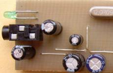
So, after we have decided on the requirements, we begin the search for details. In my bins, I found a powerful transformer TS-150-1 (it seems from a projector), which just gives out 12 and 24 V, a capacitor of 10,000 microfarads 50 V. The rest had to be purchased. So in the frame there is a transformer, a capacitor, a stabilizer chip and a harness:
After a long search for a suitable case, an Ikea napkin holder (299 rubles) was bought, which fit perfectly in size and was made of thick plastic (2 mm) and with a stainless steel lid. In the radio parts store, mortise switches, a radiator for the stabilizer, a diode bridge (at 35A) and a mechanical voltmeter for visual voltage control were also bought, so as not to resort to the services of a multimeter every time. Details in the photo:
So, some theory. As a stabilizer, it was decided to use an integral stabilizer, which, according to the principle of operation, is a linear compensation stabilizer. The industry produces many stabilizer microcircuits, both for a fixed voltage and adjustable ones. Microcircuits come in different capacities, both at 0.1 A and at 5 A or more. These microcircuits usually contain protection against a short circuit in the load. When designing a power supply, you need to decide what power the stabilizer needs, and whether it should be for a fixed voltage or adjustable. You can select the appropriate chip in the tables, for example here: http://promelec.ru/catalog_info/48/74/256/116/
Or here: http://promelec.ru/catalog_info/48/74/259/119/
Scheme of switching on an adjustable stabilizer:
Unregulated ones turn on even easier, but just in case, look in the datasheet. For my power supply, I took the KR142EN22A stabilizer at 7.5A. The only subtlety that makes it difficult to easily obtain large currents is heat dissipation. The fact is that a power equal to (Uin-Uout) * I will be dissipated by the stabilizer in the form of heat, and the possibilities for heat dissipation are very limited, therefore, to obtain large stabilized currents, you also need to change Uin, for example, I switch the transformer windings. As for the schema. C1 is selected based on 2000uF per amp of current drawn. C2-C4 is desirable to place directly next to the stabilizer. It is also recommended to connect a diode in the reverse direction in parallel with the stabilizer to protect against polarity reversal. The rest of the power supply circuit is classic.
220 volts is supplied to the primary winding of the transformer, the removed voltage from the secondary winding goes to the diode bridge, and the rectified voltage goes to a large-capacity smoothing capacitor. A stabilizer is connected to the capacitor, but the voltage can also be removed directly from the capacitor when large currents are needed and stabilization is not important. It is pointless to give specific instructions on where to solder - everything is decided based on the available details.
Here is the appearance of a handkerchief soldered to the stabilizer:
The parts are arranged in the body and all the necessary slots are made in the cover. During processing, mortise switches were replaced with toggle switches. they require less labor to install, and the stainless steel from which the lid is made is very difficult to work by hand.
All parts are installed and connected by wires. The cross section of the wires is selected based on the maximum currents. The larger the cross section, the better.
Well, a photo of the resulting power supply:
The switch on the top left is the power switch. To the right of it is the “force” mode switch that turns off the stabilizer and gives an output directly from the diode bridge (10A at 12 / 24V). Below is a 12/24 V switch for switching parts of the secondary winding. Under the voltmeter is the knob of the variable adjustment resistor. Well, the output terminals.
A lot of amateur radio power supplies (PSUs) are made on KR142EN12, KR142EN22A, KR142EN24 chips, etc. The lower adjustment limit of these microcircuits is 1.2 ... 1.3 V, but sometimes a voltage of 0.5 ... 1 V is necessary. The author offers several technical solutions for a power supply unit based on these microcircuits.
The integrated circuit (IC) KR142EN12A (Fig. 1) is an adjustable voltage regulator of the compensation type in the KT-28-2 package, which allows you to power devices with a current of up to 1.5 A in the voltage range of 1.2 ... 37 V. This integrated The stabilizer has thermally stable current protection and output short circuit protection.
Fig.1. IC KR142EN12A
Based on the IC KR142EN12A, it is possible to build an adjustable power supply, the circuit of which (without a transformer and a diode bridge) is shown in Fig. 2. The rectified input voltage is supplied from the diode bridge to the capacitor C1. Transistor VT2 and chip DA1 must be located on the radiator. The heat sink flange DA1 is electrically connected to pin 2, so if DA1 and the transistor VD2 are located on the same heatsink, they must be isolated from each other. In the author's version, DA1 is installed on a separate small heatsink, which is not galvanically connected to the heatsink and transistor VT2.

Fig.2. Adjustable PSU on IC KR142EN12A
The power dissipated by a chip with a heat sink must not exceed 10 watts. Resistors R3 and R5 form a voltage divider included in the measuring element of the stabilizer, and are selected according to the formula:
U out = U out min (1 + R3/R5).
A stabilized negative voltage of -5 V is supplied to the capacitor C2 and resistor R2 (used to select the thermally stable point VD1).
To protect against a short circuit of the output circuit of the stabilizer, it is enough to connect an electrolytic capacitor with a capacity of at least 10 μF in parallel with the resistor R3, and shunt the resistor R5 with a KD521A diode. The location of the parts is not critical, but for good temperature stability it is necessary to use the appropriate types of resistors. They should be located as far as possible from heat sources. The overall stability of the output voltage is made up of many factors and usually does not exceed 0.25% after warming up.
After turning on and warming up the device, the minimum output voltage of 0 V is set by the resistor Radd. Resistors R2 (Fig. 2) and resistor Radd (Fig. 3) must be multi-turn trimmers from the SP5 series.

Fig.3. Wiring diagram Radd
The current capabilities of the KR142EN12A microcircuit are limited to 1.5 A. Currently, microcircuits with similar parameters are on sale, but designed for a higher current in the load, for example, LM350 - for a current of 3 A, LM338 - for a current of 5 A. Data on these microcircuits can be found on the National Semiconductor website.
Recently, imported microcircuits from the LOW DROP series (SD, DV, LT1083/1084/1085) have appeared on sale. These microcircuits can operate at a reduced voltage between input and output (up to 1...1.3 V) and provide a stabilized voltage at the output in the range of 1.25...30 V at a load current of 7.5/5/3 A respectively. The closest domestic analogue of the KR142EN22 type in terms of parameters has a maximum stabilization current of 7.5 A.
At the maximum output current, the stabilization mode is guaranteed by the manufacturer at an input-output voltage of at least 1.5 V. The microcircuits also have built-in protection against exceeding the current in the load of an acceptable value and thermal protection against overheating of the case.
These stabilizers provide output voltage instability of 0.05%/V, output voltage instability when the output current changes from 10 mA to the maximum value no worse than 0.1%/V.
Figure 4 shows a power supply circuit for a home laboratory, which allows you to do without transistors VT1 and VT2, shown in Figure 2. Instead of the DA1 KR142EN12A chip, the KR142EN22A chip was used. This is an adjustable regulator with a low voltage drop, allowing you to get a current of up to 7.5 A in the load.

Fig.4. Adjustable PSU on IC KR142EN22A
The maximum power dissipation at the output of the stabilizer Pmax can be calculated by the formula:
P max \u003d (U in - U out) I out,
where U in is the input voltage supplied to the DA3 chip, U out is the output voltage at the load, I out is the output current of the microcircuit.
For example, the input voltage supplied to the microcircuit is U in \u003d 39 V, the output voltage at the load U out \u003d 30 V, the current at the load I out \u003d 5 A, then the maximum power dissipated by the microcircuit at the load is 45 W.
The electrolytic capacitor C7 is used to reduce the output impedance at high frequencies, and also lowers the noise voltage level and improves ripple smoothing. If this capacitor is tantalum, then its nominal capacitance must be at least 22 microfarads, if aluminum - at least 150 microfarads. If necessary, the capacitance of the capacitor C7 can be increased.
If the electrolytic capacitor C7 is located at a distance of more than 155 mm and is connected to the PSU with a wire with a cross section of less than 1 mm, then an additional electrolytic capacitor with a capacity of at least 10 microfarads is installed on the board parallel to the capacitor C7, closer to the microcircuit itself.
The capacitance of the filter capacitor C1 can be determined approximately, based on 2000 microfarads per 1 A of output current (at a voltage of at least 50 V). To reduce the temperature drift of the output voltage, the resistor R8 must be either wire or metal-foil with an error of no worse than 1%. Resistor R7 is the same type as R8. If the KS113A zener diode is not available, you can use the assembly shown in Fig. 3. The protection circuit solution given in the author is quite satisfied, as it works flawlessly and has been tested in practice. You can use any power supply protection circuitry, for example, those proposed in. In the author's version, when relay K1 is activated, contacts K1.1 close, shorting resistor R7, and the voltage at the PSU output becomes 0 V.
The printed circuit board of the power supply unit and the location of the elements are shown in Fig. 5, the appearance of the power supply unit is shown in Fig. 6. PCB dimensions 112x75 mm. Radiator selected needle. The DA3 chip is isolated from the heatsink by a gasket and attached to it with a steel spring plate that presses the chip to the heatsink.


Fig.5. PSU circuit board and element layout
Capacitor C1 of type K50-24 is composed of two capacitors connected in parallel with a capacity of 4700 μFx50 V. An imported analog of a capacitor of type K50-6 with a capacity of 10,000 μFx50 V can be used. The capacitor should be located as close as possible to the board, and the conductors connecting it to the board should be as short as possible. Capacitor C7 manufactured by Weston with a capacity of 1000 uFx50 V. Capacitor C8 is not shown in the diagram, but there are holes on the printed circuit board for it. You can use a capacitor with a rating of 0.01 ... 0.1 μF for a voltage of at least 10 ... 15 V.

Fig.6. PSU appearance
Diodes VD1-VD4 are an imported RS602 diode microassembly, designed for a maximum current of 6 A (Fig. 4). The RES10 relay (passport RS4524302) is used in the power supply protection circuit. In the author's version, a resistor R7 of the SPP-ZA type was used with a parameter spread of no more than 5%. Resistor R8 (Fig. 4) must have a spread of no more than 1% from the specified value.
The power supply usually does not require configuration and starts working immediately after assembly. After warming up the unit with resistor R6 (Fig. 4) or resistor Rdop (Fig. 3), 0 V is set at the nominal value of R7.
In this design, a power transformer of the OSM-0.1UZ brand with a power of 100 W is used. Magnetic core ShL25/40-25. The primary winding contains 734 turns of PEV wire 0.6 mm, winding II - 90 turns of PEV wire 1.6 mm, winding III - 46 turns of PEV wire 0.4 mm with a tap from the middle.
The RS602 diode assembly can be replaced with diodes rated for a current of at least 10 A, for example, KD203A, V, D or KD210 A-G (if you do not place the diodes separately, you will have to redo the printed circuit board). As a transistor VT1, you can use the transistor KT361G.
Sources:
- http://www.national.com/catalog/AnalogRegulators_LinearRegulators-StandardNPN_PositiveVoltageAdjutable.html
- Morokhin L. Laboratory power supply//Radio. - 1999 - No. 2
- Nechaev I. Protection of small network power supplies from overloads//Radio. - 1996.-№12
List of radio elements
| Designation | A type | Denomination | Quantity | Note | Score | My notepad | |
|---|---|---|---|---|---|---|---|
| DA1 | Linear Regulator | LM78L12 | 1 | To notepad | |||
| VT1 | bipolar transistor | KT814G | 1 | To notepad | |||
| VT2 | bipolar transistor | KT819G | 1 | To notepad | |||
| VD1 | zener diode | KS113A | 1 | To notepad | |||
| C1 | 4700uF 50V | 1 | To notepad | ||||
| C2 | Capacitor | 0.1uF | 1 | To notepad | |||
| C3 | electrolytic capacitor | 47uF 50V | 1 | To notepad | |||
| R1 | Resistor | 2.2 ohm | 1 | 1 W | To notepad | ||
| R2 | Trimmer resistor | 470 ohm | 1 | To notepad | |||
| R3 | Variable resistor | 2.2 kOhm | 1 | To notepad | |||
| R4 | Resistor | 240 ohm | 1 | 2 W | To notepad | ||
| R5 | Resistor | 91 ohm | 1 | 1 W | To notepad | ||
| C2 | Capacitor | 0.1uF | 1 | To notepad | |||
| R2 | Resistor | 210 ohm | 1 | To notepad | |||
| R ext. | Trimmer resistor | 470 ohm | 1 | To notepad | |||
| DA1 | Linear Regulator | LM7805 | 1 | To notepad | |||
| DA2 | Linear Regulator | LM79L05 | 1 | To notepad | |||
| DA3 | Linear Regulator | LT1083 | 1 | KR142EN22A | To notepad | ||
| VT1 | bipolar transistor | KT203A | 1 | To notepad | |||
| VD1-VD4 | Diode bridge | RS602 | 1 | To notepad | |||
| VD5-VD8 | Diode bridge | KTS407A | 1 | To notepad | |||
| VD9, VD10 | Diode | KD522B | 2 | To notepad | |||
| VD11 | zener diode | KS113A | 1 | To notepad | |||
| VS1 | Thyristor | KU103E | 1 | To notepad | |||
| C1 | electrolytic capacitor | 10000uF 50V | 1 | To notepad | |||
| C2, C3 | electrolytic capacitor | 470uF 25V | 2 | To notepad | |||
| C4, C5 | electrolytic capacitor | 22uF 16V | 2 | To notepad | |||
| C6 | Capacitor | 0.1uF | 1 | To notepad | |||
| C7 | electrolytic capacitor | 1000uF 50V | 1 | To notepad | |||
| R1 | Resistor | ||||||
A lot of amateur radio power supplies (PSUs) are made on KR142EN12, KR142EN22A, KR142EN24 chips, etc. The lower adjustment limit of these microcircuits is 1.2 ... 1.3 V, but sometimes a voltage of 0.5 ... 1 V is necessary. The author offers several technical solutions for a power supply unit based on these microcircuits.
The integrated circuit (IC) KR142EN12A (Fig. 1) is an adjustable voltage regulator of the compensation type in the KT-28-2 package, which allows you to power devices with a current of up to 1.5 A in the voltage range of 1.2 ... 37 V. This integrated The stabilizer has thermally stable current protection and output short circuit protection.
Fig.1. IC KR142EN12A
Based on the IC KR142EN12A, it is possible to build an adjustable power supply, the circuit of which (without a transformer and a diode bridge) is shown in Fig. 2. The rectified input voltage is supplied from the diode bridge to the capacitor C1. Transistor VT2 and chip DA1 must be located on the radiator. The heat sink flange DA1 is electrically connected to pin 2, so if DA1 and the transistor VD2 are located on the same heatsink, they must be isolated from each other. In the author's version, DA1 is installed on a separate small heatsink, which is not galvanically connected to the heatsink and transistor VT2.

Fig.2. Adjustable PSU on IC KR142EN12A
The power dissipated by a chip with a heat sink must not exceed 10 watts. Resistors R3 and R5 form a voltage divider included in the measuring element of the stabilizer, and are selected according to the formula:
U out = U out min (1 + R3/R5).
A stabilized negative voltage of -5 V is supplied to the capacitor C2 and resistor R2 (used to select the thermally stable point VD1).
To protect against a short circuit of the output circuit of the stabilizer, it is enough to connect an electrolytic capacitor with a capacity of at least 10 μF in parallel with the resistor R3, and shunt the resistor R5 with a KD521A diode. The location of the parts is not critical, but for good temperature stability it is necessary to use the appropriate types of resistors. They should be located as far as possible from heat sources. The overall stability of the output voltage is made up of many factors and usually does not exceed 0.25% after warming up.
After turning on and warming up the device, the minimum output voltage of 0 V is set by the resistor Radd. Resistors R2 (Fig. 2) and resistor Radd (Fig. 3) must be multi-turn trimmers from the SP5 series.

Fig.3. Wiring diagram Radd
The current capabilities of the KR142EN12A microcircuit are limited to 1.5 A. Currently, microcircuits with similar parameters are on sale, but designed for a higher current in the load, for example, LM350 - for a current of 3 A, LM338 - for a current of 5 A. Data on these microcircuits can be found on the National Semiconductor website.
Recently, imported microcircuits from the LOW DROP series (SD, DV, LT1083/1084/1085) have appeared on sale. These microcircuits can operate at a reduced voltage between input and output (up to 1...1.3 V) and provide a stabilized voltage at the output in the range of 1.25...30 V at a load current of 7.5/5/3 A respectively. The closest domestic analogue of the KR142EN22 type in terms of parameters has a maximum stabilization current of 7.5 A.
At the maximum output current, the stabilization mode is guaranteed by the manufacturer at an input-output voltage of at least 1.5 V. The microcircuits also have built-in protection against exceeding the current in the load of an acceptable value and thermal protection against overheating of the case.
These stabilizers provide output voltage instability of 0.05%/V, output voltage instability when the output current changes from 10 mA to the maximum value no worse than 0.1%/V.
Figure 4 shows a power supply circuit for a home laboratory, which allows you to do without transistors VT1 and VT2, shown in Figure 2. Instead of the DA1 KR142EN12A chip, the KR142EN22A chip was used. This is an adjustable regulator with a low voltage drop, allowing you to get a current of up to 7.5 A in the load.

Fig.4. Adjustable PSU on IC KR142EN22A
The maximum power dissipation at the output of the stabilizer Pmax can be calculated by the formula:
P max \u003d (U in - U out) I out,
where U in is the input voltage supplied to the DA3 chip, U out is the output voltage at the load, I out is the output current of the microcircuit.
For example, the input voltage supplied to the microcircuit is U in \u003d 39 V, the output voltage at the load U out \u003d 30 V, the current at the load I out \u003d 5 A, then the maximum power dissipated by the microcircuit at the load is 45 W.
The electrolytic capacitor C7 is used to reduce the output impedance at high frequencies, and also lowers the noise voltage level and improves ripple smoothing. If this capacitor is tantalum, then its nominal capacitance must be at least 22 microfarads, if aluminum - at least 150 microfarads. If necessary, the capacitance of the capacitor C7 can be increased.
If the electrolytic capacitor C7 is located at a distance of more than 155 mm and is connected to the PSU with a wire with a cross section of less than 1 mm, then an additional electrolytic capacitor with a capacity of at least 10 microfarads is installed on the board parallel to the capacitor C7, closer to the microcircuit itself.
The capacitance of the filter capacitor C1 can be determined approximately, based on 2000 microfarads per 1 A of output current (at a voltage of at least 50 V). To reduce the temperature drift of the output voltage, the resistor R8 must be either wire or metal-foil with an error of no worse than 1%. Resistor R7 is the same type as R8. If the KS113A zener diode is not available, you can use the assembly shown in Fig. 3. The protection circuit solution given in the author is quite satisfied, as it works flawlessly and has been tested in practice. You can use any power supply protection circuitry, for example, those proposed in. In the author's version, when relay K1 is activated, contacts K1.1 close, shorting resistor R7, and the voltage at the PSU output becomes 0 V.
The printed circuit board of the power supply unit and the location of the elements are shown in Fig. 5, the appearance of the power supply unit is shown in Fig. 6. PCB dimensions 112x75 mm. Radiator selected needle. The DA3 chip is isolated from the heatsink by a gasket and attached to it with a steel spring plate that presses the chip to the heatsink.


Fig.5. PSU circuit board and element layout
Capacitor C1 of type K50-24 is composed of two capacitors connected in parallel with a capacity of 4700 μFx50 V. An imported analog of a capacitor of type K50-6 with a capacity of 10,000 μFx50 V can be used. The capacitor should be located as close as possible to the board, and the conductors connecting it to the board should be as short as possible. Capacitor C7 manufactured by Weston with a capacity of 1000 uFx50 V. Capacitor C8 is not shown in the diagram, but there are holes on the printed circuit board for it. You can use a capacitor with a rating of 0.01 ... 0.1 μF for a voltage of at least 10 ... 15 V.

Fig.6. PSU appearance
Diodes VD1-VD4 are an imported RS602 diode microassembly, designed for a maximum current of 6 A (Fig. 4). The RES10 relay (passport RS4524302) is used in the power supply protection circuit. In the author's version, a resistor R7 of the SPP-ZA type was used with a parameter spread of no more than 5%. Resistor R8 (Fig. 4) must have a spread of no more than 1% from the specified value.
The power supply usually does not require configuration and starts working immediately after assembly. After warming up the unit with resistor R6 (Fig. 4) or resistor Rdop (Fig. 3), 0 V is set at the nominal value of R7.
In this design, a power transformer of the OSM-0.1UZ brand with a power of 100 W is used. Magnetic core ShL25/40-25. The primary winding contains 734 turns of PEV wire 0.6 mm, winding II - 90 turns of PEV wire 1.6 mm, winding III - 46 turns of PEV wire 0.4 mm with a tap from the middle.
The RS602 diode assembly can be replaced with diodes rated for a current of at least 10 A, for example, KD203A, V, D or KD210 A-G (if you do not place the diodes separately, you will have to redo the printed circuit board). As a transistor VT1, you can use the transistor KT361G.
Sources
- http://www.national.com/catalog/AnalogRegulators_LinearRegulators-StandardNPN_PositiveVoltageAdjutable.html
- Morokhin L. Laboratory power supply//Radio. - 1999 - No. 2
- Nechaev I. Protection of small network power supplies from overloads//Radio. - 1996.-№12
Publication date: 25.04.2005
Readers' opinions
- Ivan / 21.02.2017 - 01:33
Please tell me how to make a block for the car radio - Kuzmich / 12/14/2012 - 10:34
Dimensions are not critical for me. The scheme is good, I will repeat. When you are engaged in the repair of any household crap - that's it. - LipGard / 26.10.2012 - 05:48
I'm a noob at this so far, I want to understand. And how to regulate the voltage of the PSU, probably R7? Is there any way to display it on the panel? And perhaps you can connect a voltmeter to see the voltage at the output? It probably needs to be connected to the output)? Can the current be regulated? - Vasya / 08.09.2012 - 12:41
Well, why did someone else fart something or not. But the scheme is really cool - Oleg / 04.02.2012 - 20:25
When repairing radio stations, it is better to use trances, there is no HF interference from them. - dd / 25.11.2011 - 05:54
the circuit in Figure 2 deserves attention and some impulses will not replace it in amateur conditions, nonsense is better to make transformers simpler and more reliable and remotto-suitable - / 06.05.2011 - 19:49
fuck you build an inverter - dimon / 05/06/2011 - 19:43
Haven't you seen the diagram? - spkpk / 05.05.2011 - 08:09
speckrn - olzhas / 12.09.2010 - 08:40
power supply - Eugene / 06/02/2010 - 07:09
Yes, pulsers are better, but a conventional transformer power supply is more suitable for laboratory research. - Mercury / 10/19/2009 - 07:51
It is better to make switching power supplies. And this is all nonsense ... provided that you do not need to do some kind of galvanic isolation. If there are no such requirements, then impulses are better. The dimensions are much smaller!