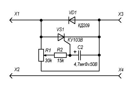
Triac power regulator. Rectifiers with thyristor voltage regulator To 125 12 5 application
(Option 1)
In triac power regulators operating on the principle of passing a certain number of current half-cycles per unit time through the load, the condition of evenness of their number must be met. In many well-known amateur radio (and not only) designs it is violated. Readers are offered a regulator that is free from this drawback. Its diagram is shown in rice. 1.
There is a power supply unit, an adjustable duty cycle pulse generator and a pulse shaper that controls the triac. The power supply unit is made according to the classical scheme: current-limiting resistor R2 and capacitor C1, rectifier on diodes VD3, VD4, zener diode VD5, smoothing capacitor SZ. The pulse frequency of the generator, assembled on elements DD1.1, DD1.2 and DD1.4, depends on the capacitance of capacitor C2 and the resistance between the extreme terminals of variable resistor R1. The same resistor regulates the duty cycle of the pulses. Element DD1.3 serves as a pulse generator with the frequency of the mains voltage supplied to its output 1 through a divider of resistors R3 and R4, and each pulse begins near the transition of the instantaneous value of the mains voltage through zero. From the output of element DD1.3, these pulses through limiting resistors R5 and R6 arrive at the bases of transistors VT1, VT2. The control pulses amplified by the transistors come through the separating capacitor C4 to the control electrode of the triac VS1. Here their polarity corresponds to the sign of the mains voltage applied at that moment to the pin. 2 triacs. Due to the fact that elements DD1.1 and DD1.2, DD1.3 and DD1.4 form two triggers, the level at the output of element DD1.4, connected to pin 2 of element DD1.3, changes to the opposite only in the negative half-cycle of the mains voltage . Suppose the trigger on elements DD1.3, DD1.4 is in a state with a low level at the output of element DD1.3 and a high level at the output of element DD1.4. To change this state, it is necessary that the high level at the output of element DD1.2, connected to pin 6 of element DD1.4, becomes low. And this can only happen in the negative half-cycle of the mains voltage supplied to pin 13 of element DD1.1, regardless of the moment the high level is set at pin 8 of element DD1.2. The formation of a control pulse begins with the arrival of a positive half-cycle of the mains voltage at pin 1 of element DD1.3. At some point, as a result of recharging capacitor C2, the high level at pin 8 of element DD1.2 will change to low, which will set a high voltage level at the output of the element. Now the high level at the output of element DD1.4 can also change to low, but only during the negative half-cycle of the voltage supplied to pin 1 of element DD1.3. Consequently, the operating cycle of the control pulse shaper will end at the end of the negative half-cycle of the mains voltage, and the total number of half-cycles of the voltage applied to the load will be even. The main part of the device parts is mounted on a board with single-sided printing, the drawing of which is shown in rice. 2.
Diodes VD1 and VD2 are soldered directly to the terminals of variable resistor R1, and resistor R7 is soldered to the terminals of triac VS1. The triac is equipped with a factory-made ribbed heat sink with a heat-removing surface area of about 400 cm2. Fixed resistors MLT were used, variable resistor R1 - SPZ-4aM. It can be replaced by another of the same or greater resistance. The values of resistors R3 and R4 must be the same. Capacitors C1, C2 - K73-17. If increased reliability is required, then the oxide capacitor C4 can be replaced with a film capacitor, for example, K73-17 2.2...4.7 μF at 63 V, but the size of the printed circuit board will have to be increased.
Instead of KD521A diodes, other low-power silicon ones will also be suitable, and the D814V zener diode will replace any more modern one with a stabilization voltage of 9 V. Replacing transistors KT3102V, KT3107G - other low-power silicon ones of the corresponding structure. If the amplitude of the current pulses opening the triac VS1 is insufficient, the resistance of resistors R5 and R6 cannot be reduced. It is better to select transistors with the highest possible current transfer coefficient at a voltage between the collector and emitter of 1 V. For VT1 it should be 150...250, for VT2 - 250...270. Upon completion of installation, you can connect a load with a resistance of 50...100 Ohms to the regulator and connect it to the network. Connect a 300...600 V DC voltmeter in parallel to the load. If the triac opens steadily in both half-cycles of the mains voltage, the voltmeter needle does not deviate from zero at all or fluctuates slightly around it. If the voltmeter needle deviates only in one direction, it means that the triac opens only in half-cycles of the same sign. The direction of deflection of the arrow corresponds to the polarity of the voltage applied to the triac at which it remains closed. Usually, correct operation of the triac can be achieved by installing transistor VT2 with a high current transfer coefficient.
Triac power regulator.
(Option 2)
The proposed triac power regulator (see figure) can be used to regulate the active power of heating devices (soldering iron, electric stove, stove, etc.). It is not recommended to use it to change the brightness of lighting fixtures, because they will flash heavily. A special feature of the regulator is the switching of the triac when the mains voltage crosses zero, so it does not create network interference. The power is regulated by changing the number of half-cycles of the mains voltage supplied to the load.
The synchronizer is made on the basis of the logical element EXCLUSIVE OR DD1.1. Its feature is the appearance of a high level (logical “1”) at the output in the case when the input signals differ from each other, and a low level (“O”) when the input signals coincide. As a result of this, "G appears at the DD1.1 output only when the mains voltage crosses zero. The rectangular pulse generator with adjustable duty cycle is made on logic elements DD1.2 and DD1.3. Connecting one of the inputs of these elements to power turns them into inverters The result is a square pulse generator.The pulse frequency is approximately 2 Hz, and their duration is changed by resistor R5.

On resistor R6 and diodes VD5. VD6 has a 2I matching circuit. A high level at its output appears only when two “1”s coincide (the synchronization pulse and the pulse from the generator). As a result, bursts of synchronization pulses appear at output 11 DD1.4. Element DD1.4 is a pulse repeater, for which one of its inputs is connected to a common bus.
Transistor VT1 contains a control pulse shaper. Packs of short pulses from its emitter, synchronized with the beginning of half-cycles of the mains voltage, arrive at the control transition of triac VS1 and open it. Current flows through RH.
The triac power regulator is powered through the R1-C1-VD2 chain. Zener diode VD1 limits the supply voltage to 15 V. Positive pulses from zener diode VD1 through diode VD2 charge capacitor SZ.
With high regulated power, triac VS1 must be installed on a radiator. Then a triac of the KU208G type allows you to switch power up to 1 kW. The dimensions of the radiator can be approximately estimated from the calculation that for 1 W of dissipated power, about 10 cm2 of the effective surface of the radiator is required (the triac body itself dissipates 10 W of power). For more power, a more powerful triac is needed, for example, TS2-25-6. It allows you to switch a current of 25 A. The triac is selected with a permissible reverse voltage of at least 600 V. It is advisable to protect the triac with a varistor connected in parallel, for example, CH-1-1-560. Diodes VD2...VD6 can be used in any circuit, for example. KD522B or KD510A Zener diode - any low-power voltage 14...15 V. D814D will do.
The triac power regulator is placed on a printed circuit board made of single-sided fiberglass with dimensions of 68x38 mm.
Simple power regulator.
Power regulator up to 1 kW (0%-100%).
The circuit has been assembled more than once and works without adjustment or other problems. Naturally, diodes and a thyristor for a radiator with a power of more than 300 watts. If less, then the housings of the parts themselves are enough for cooling.
Initially, the circuit used transistors such as MP38 and MP41.
The scheme proposed below will reduce the power of any heating electrical appliance. The circuit is quite simple and accessible even to a novice radio amateur. To control a more powerful load, thyristors must be placed on a radiator (150 cm2 or more). To eliminate interference created by the regulator, it is advisable to install a choke at the input.
On the parent circuit, a KU208G triac was installed, and I was not satisfied with it due to the low switching power. After some digging I found imported triacs BTA16-600. The maximum switching voltage of which is 600 volts at a current of 16A!!!
All MLT resistors are 0.125;
R4 - SP3-4aM;
The capacitor is made up of two (connected in parallel) 1 microfarad of 250 volts, type K73-17.
With the data indicated in the diagram, the following results were achieved: Voltage adjustment from 40 to mains voltage.
The regulator can be inserted into the standard heater housing.
The circuit is copied from the vacuum cleaner regulator board.

Marking on the condenser: 1j100
I tried to control a 2 kW heating element - I didn’t notice any blinking of the light in the same phase,
the voltage on the heating element is regulated smoothly and seemingly uniformly (proportional to the angle of rotation of the resistor).
Adjustable from 0 to 218 volts with a network voltage of 224-228 volts.
The article describes how a thyristor power regulator works, the diagram of which will be presented below
In everyday life, very often there is a need to regulate the power of household appliances, such as electric stoves, soldering irons, boilers and heating elements, in transport - engine speed, etc. The simplest amateur radio design comes to the rescue - a power regulator on a thyristor. Assembling such a device will not be difficult; it can become the very first home-made device that will perform the function of adjusting the temperature of the soldering iron tip of a novice radio amateur. It is worth noting that ready-made soldering stations with temperature control and other nice functions are an order of magnitude more expensive than a simple soldering iron. A minimal set of parts allows you to assemble a simple thyristor power regulator for wall mounting.
For your information, surface mounting is a method of assembling radio-electronic components without using a printed circuit board, and with good skill it allows you to quickly assemble electronic devices of medium complexity.
You can also order a thyristor regulator, and for those who want to figure it out on their own, a diagram will be presented below and the principle of operation will be explained.
By the way, this is a single-phase thyristor power regulator. Such a device can be used to control power or speed. However, first we need to understand this because this will allow us to understand for what load it is better to use such a regulator.
How does a thyristor work?
A thyristor is a controlled semiconductor device capable of conducting current in one direction. The word “controlled” was used for a reason, because with its help, unlike a diode, which also conducts current only to one pole, you can select the moment when the thyristor begins to conduct current. The thyristor has three outputs:
- Anode.
- Cathode.
- Control electrode.

In order for current to begin flowing through the thyristor, the following conditions must be met: the part must be in a circuit that is energized, and a short-term pulse must be applied to the control electrode. Unlike a transistor, controlling a thyristor does not require holding the control signal. The nuances do not end there: the thyristor can be closed only by interrupting the current in the circuit, or by generating a reverse anode-cathode voltage. This means that the use of a thyristor in DC circuits is very specific and often unwise, but in AC circuits, for example in a device such as a thyristor power regulator, the circuit is constructed in such a way that a condition for closing is ensured. Each of the half-waves will close the corresponding thyristor.
Most likely, you don’t understand everything? Do not despair - below the process of operation of the finished device will be described in detail.
Scope of application of thyristor regulators
In what circuits is it effective to use a thyristor power regulator? The circuit allows you to perfectly regulate the power of heating devices, that is, influence the active load. When working with a highly inductive load, the thyristors may simply not close, which can lead to failure of the regulator.
Is it possible to have an engine?
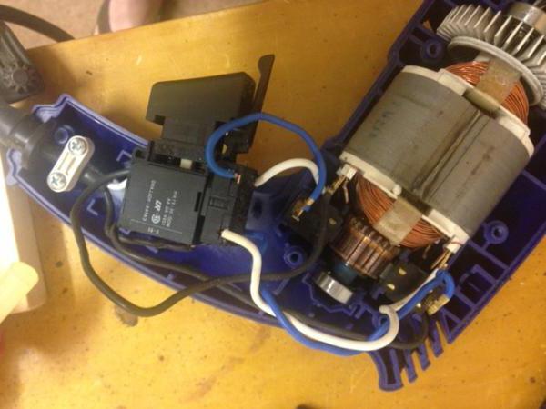
I think many of the readers have seen or used drills, angle grinders, which are popularly called “grinders,” and other power tools. You may have noticed that the number of revolutions depends on the depth of pressing the trigger button of the device. It is in this element that a thyristor power regulator is built in (the diagram of which is shown below), with the help of which the number of revolutions is changed.
Note! The thyristor regulator cannot change the speed of asynchronous motors. Thus, the voltage is regulated on commutator motors equipped with a brush assembly.
Scheme of one and two thyristors
A typical circuit for assembling a thyristor power regulator with your own hands is shown in the figure below.

The output voltage of this circuit is from 15 to 215 volts; in the case of using the indicated thyristors installed on heat sinks, the power is about 1 kW. By the way, the switch with the light brightness control is made according to a similar scheme.
If you don't need to fully regulate the voltage and just want an output of 110 to 220 volts, use this diagram, which shows a half-wave thyristor power regulator.
How it works?

The information described below is valid for most schemes. Letter designations will be taken in accordance with the first circuit of the thyristor regulator
A thyristor power regulator, the operating principle of which is based on phase control of the voltage value, also changes the power. This principle lies in the fact that under normal conditions the load is affected by the alternating voltage of the household network, changing according to a sinusoidal law. Above, when describing the operating principle of a thyristor, it was said that each thyristor operates in one direction, that is, it controls its own half-wave from a sine wave. What does it mean?
If you periodically connect a load using a thyristor at a strictly defined moment, the value of the effective voltage will be lower, since part of the voltage (the effective value that “falls” on the load) will be less than the mains voltage. This phenomenon is illustrated in the graph.
The shaded area is the area of stress that is under load. The letter “a” on the horizontal axis indicates the opening moment of the thyristor. When the positive half-wave ends and the period with the negative half-wave begins, one of the thyristors closes, and at the same moment the second thyristor opens.
Let's figure out how our specific thyristor power regulator works
Scheme one
Let us stipulate in advance that instead of the words “positive” and “negative”, “first” and “second” (half-wave) will be used.
So, when the first half-wave begins to act on our circuit, capacitors C1 and C2 begin to charge. Their charging speed is limited by potentiometer R5. this element is variable, and with its help the output voltage is set. When the voltage necessary to open dinistor VS3 appears on capacitor C1, the dinistor opens and current flows through it, with the help of which thyristor VS1 will be opened. The moment of breakdown of the dinistor is point “a” on the graph presented in the previous section of the article. When the voltage value passes through zero and the circuit is under the second half-wave, the thyristor VS1 closes, and the process is repeated again, only for the second dinistor, thyristor and capacitor. Resistors R3 and R3 are used for control, and R1 and R2 are used for thermal stabilization of the circuit.
The principle of operation of the second circuit is similar, but it controls only one of the half-waves of alternating voltage. Now, knowing the principle of operation and the circuit, you can assemble or repair a thyristor power regulator with your own hands.
Using the regulator in everyday life and safety precautions

It must be said that this circuit does not provide galvanic isolation from the network, so there is a danger of electric shock. This means that you should not touch the regulator elements with your hands. An insulated housing must be used. You should design the design of your device so that, if possible, you can hide it in an adjustable device and find free space in the case. If the adjustable device is located permanently, then in general it makes sense to connect it through a switch with a dimmer. This solution will partially protect against electric shock, eliminate the need to find a suitable housing, and has an attractive appearance and manufactured industrially.
When developing an adjustable power supply without a high-frequency converter, the developer is faced with the problem that with a minimum output voltage and a large load current, the stabilizer dissipates a lot of power on the regulating element. Until now, in most cases, this problem was solved this way: they made several taps at the secondary winding of the power transformer and divided the entire output voltage adjustment range into several subranges. This principle is used in many serial power supplies, for example, UIP-2 and more modern ones. It is clear that the use of a power supply with multiple subbands becomes more complex, and so does remote control such a power source, for example, from a computer.
It seemed to me that the solution was to use a controlled rectifier on a thyristor, since it becomes possible to create a power source controlled by one knob for setting the output voltage or by one control signal with an output voltage adjustment range from zero (or almost from zero) to the maximum value. Such a power source could be made from commercially available parts.
To date, controlled rectifiers with thyristors have been described in great detail in books on power supplies, but in practice they are rarely used in laboratory power supplies. They are also rarely found in amateur designs (except, of course, chargers for car batteries). I hope that this work will help change this state of affairs.
In principle, the circuits described here can be used to stabilize the input voltage of a high-frequency converter, for example, as is done in the “Electronics Ts432” TVs. The circuits shown here can also be used to make laboratory power supplies or chargers.
I give a description of my work not in the order in which I carried it out, but in a more or less orderly manner. Let's look at general issues first, then “low-voltage” designs such as power supplies for transistor circuits or charging batteries, and then “high-voltage” rectifiers for powering vacuum tube circuits.
Operation of a thyristor rectifier with a capacitive load
The literature describes a large number of thyristor power regulators operating on alternating or pulsating current with a resistive (for example, incandescent lamps) or inductive (for example, an electric motor) load. The rectifier load is usually a filter in which capacitors are used to smooth out ripples, so the rectifier load can be capacitive in nature.
Let's consider the operation of a rectifier with a thyristor regulator for a resistive-capacitive load. A diagram of such a regulator is shown in Fig. 1.
Rice. 1.
Here, as an example, a full-wave rectifier with a midpoint is shown, but it can also be made using another circuit, for example, a bridge. Sometimes thyristors, in addition to regulating the voltage at the load U n They also perform the function of rectifier elements (valves), however, this mode is not allowed for all thyristors (KU202 thyristors with some letters allow operation as valves). For clarity of presentation, we assume that thyristors are used only to regulate the voltage across the load U n , and straightening is performed by other devices.
The operating principle of a thyristor voltage regulator is illustrated in Fig. 2. At the output of the rectifier (the connection point of the cathodes of the diodes in Fig. 1), voltage pulses are obtained (the lower half-wave of the sine wave is “turned” up), indicated U rect . Ripple frequency f p at the output of the full-wave rectifier is equal to twice the network frequency, i.e. 100 Hz when powered from mains 50 Hz . The control circuit supplies current pulses (or light if an optothyristor is used) with a certain delay to the thyristor control electrode t z relative to the beginning of the pulsation period, i.e. the moment when the rectifier voltage U rect becomes equal to zero.

Rice. 2.
Figure 2 is for the case where the delay t z exceeds half the pulsation period. In this case, the circuit operates on the incident section of a sine wave. The longer the delay when the thyristor is turned on, the lower the rectified voltage will be. U n on load. Load voltage ripple U n smoothed by filter capacitor C f . Here and below, some simplifications are made when considering the operation of the circuits: the output resistance of the power transformer is considered equal to zero, the voltage drop across the rectifier diodes is not taken into account, and the thyristor turn-on time is not taken into account. It turns out that recharging the filter capacity C f happens as if instantly. In reality, after applying a trigger pulse to the control electrode of the thyristor, charging the filter capacitor takes some time, which, however, is usually much less than the pulsation period T p.
Now imagine that the delay in turning on the thyristor t z equal to half the pulsation period (see Fig. 3). Then the thyristor will turn on when the voltage at the rectifier output passes through the maximum.

Rice. 3.
In this case, the load voltage U n will also be the largest, approximately the same as if there were no thyristor regulator in the circuit (we neglect the voltage drop across the open thyristor).
This is where we run into a problem. Let's assume that we want to regulate the load voltage from almost zero to the highest value that can be obtained from the existing power transformer. To do this, taking into account the assumptions made earlier, it will be necessary to apply trigger pulses to the thyristor EXACTLY at the moment when U rect passes through a maximum, i.e. t z = T p /2. Taking into account the fact that the thyristor does not open instantly, but recharging the filter capacitor C f also requires some time, the triggering pulse must be submitted somewhat EARLIER than half the pulsation period, i.e. t z< T п /2. The problem is that, firstly, it is difficult to say how much earlier, since it depends on factors that are difficult to accurately take into account when calculating, for example, the turn-on time of a given thyristor instance or the total (taking into account inductances) output resistance of the power transformer. Secondly, even if the circuit is calculated and adjusted absolutely accurately, the turn-on delay time t z , network frequency, and therefore frequency and period T p ripples, thyristor turn-on time and other parameters may change over time. Therefore, in order to obtain the highest voltage at the load U n there is a desire to turn on the thyristor much earlier than half the pulsation period.
Let's assume that we did just that, i.e. we set the delay time t z much less T p /2. Graphs characterizing the operation of the circuit in this case are shown in Fig. 4. Note that if the thyristor opens before half the half cycle, it will remain in the open state until the process of charging the filter capacitor is completed C f (see the first pulse in Fig. 4).

Rice. 4.
It turns out that for a short delay time t z fluctuations in the output voltage of the regulator may occur. They occur if, at the moment the trigger pulse is applied to the thyristor, the voltage on the load U n there is more voltage at the output of the rectifier U rect . In this case, the thyristor is under reverse voltage and cannot open under the influence of a trigger pulse. One or more trigger pulses may be missed (see second pulse in Figure 4). The next turn on of the thyristor will occur when the filter capacitor is discharged and at the moment the control pulse is applied, the thyristor will be under direct voltage.
Probably the most dangerous case is when every second pulse is missed. In this case, a direct current will pass through the winding of the power transformer, under the influence of which the transformer may fail.
In order to avoid the appearance of an oscillatory process in the thyristor regulator circuit, it is probably possible to abandon pulse control of the thyristor, but in this case the control circuit becomes more complicated or becomes uneconomical. Therefore, the author developed a thyristor regulator circuit in which the thyristor is normally triggered by control pulses and no oscillatory process occurs. Such a diagram is shown in Fig. 5.

Rice. 5.
Here the thyristor is loaded onto the starting resistance R p , and the filter capacitor C R n connected via starting diode VD p . In such a circuit, the thyristor starts up regardless of the voltage on the filter capacitor C f .After applying a trigger pulse to the thyristor, its anode current first begins to pass through the trigger resistance R p and then when the voltage is on R p will exceed the load voltage U n , the starting diode opens VD p and the anode current of the thyristor recharges the filter capacitor C f . Resistance R p such a value is selected to ensure stable startup of the thyristor with a minimum delay time of the trigger pulse t z . It is clear that some power is uselessly lost at the starting resistance. Therefore, in the above circuit, it is preferable to use thyristors with a low holding current, then it will be possible to use a large starting resistance and reduce power losses.
Scheme in Fig. 5 has the disadvantage that the load current passes through an additional diode VD p , at which part of the rectified voltage is uselessly lost. This drawback can be eliminated by connecting a starting resistor R p to a separate rectifier. Circuit with a separate control rectifier, from which the starting circuit and starting resistance are powered R p shown in Fig. 6. In this circuit, the control rectifier diodes can be low-power since the load current flows only through the power rectifier.

Rice. 6.
Low voltage power supplies with thyristor regulator
Below is a description of several designs of low-voltage rectifiers with a thyristor regulator. When making them, I took as a basis the circuit of a thyristor regulator used in devices for charging car batteries (see Fig. 7). This scheme was successfully used by my late comrade A.G. Spiridonov.

Rice. 7.
The elements circled in the diagram (Fig. 7) were installed on a small printed circuit board. Several similar schemes are described in the literature; the differences between them are minimal, mainly in the types and ratings of parts. The main differences are:
1. Timing capacitors of different capacities are used, i.e. instead of 0.5m F put 1 m F , and, accordingly, a variable resistance of a different value. To reliably start the thyristor in my circuits, I used a 1 capacitorm F.
2. In parallel with the timing capacitor, you do not need to install a resistance (3 k Win Fig. 7). It is clear that in this case a variable resistance may not be required by 15 k W, and of a different magnitude. I have not yet found out the influence of the resistance parallel to the timing capacitor on the stability of the circuit.
3. Most of the circuits described in the literature use transistors of the KT315 and KT361 types. Sometimes they fail, so in my circuits I used more powerful transistors types KT816 and KT817.
4. To base connection point pnp and npn collector transistors, a divider of resistances of a different value can be connected (10 k W and 12 k W in Fig. 7).
5. A diode can be installed in the thyristor control electrode circuit (see the diagrams below). This diode eliminates the influence of the thyristor on the control circuit.
The diagram (Fig. 7) is given as an example; several similar diagrams with descriptions can be found in the book “Chargers and Start-Chargers: Information Review for Car Enthusiasts / Comp. A. G. Khodasevich, T. I. Khodasevich -M.:NT Press, 2005.” The book consists of three parts, it contains almost all chargers in the history of mankind.
The simplest circuit of a rectifier with a thyristor voltage regulator is shown in Fig. 8.

Rice. 8.
This circuit uses a full-wave midpoint rectifier because it contains fewer diodes, so fewer heatsinks are needed and higher efficiency. The power transformer has two secondary windings for alternating voltage 15 V . The thyristor control circuit here consists of capacitor C1, resistances R 1- R 6, transistors VT 1 and VT 2, diode VD 3.
Let's consider the operation of the circuit. Capacitor C1 is charged through a variable resistance R 2 and constant R 1. When the voltage on the capacitor C 1 will exceed the voltage at the point of resistance connection R 4 and R 5, transistor opens VT 1. Transistor collector current VT 1 opens VT 2. In turn, the collector current VT 2 opens VT 1. Thus, the transistors open like an avalanche and the capacitor discharges C 1 V thyristor control electrode VS 1. This creates a triggering impulse. Changing by variable resistance R 2 trigger pulse delay time, the output voltage of the circuit can be adjusted. The greater this resistance, the slower the capacitor charges. C 1, the trigger pulse delay time is longer and the output voltage at the load is lower.
Constant resistance R 1, connected in series with variable R 2 limits the minimum pulse delay time. If it is greatly reduced, then at the minimum position of the variable resistance R 2, the output voltage will disappear abruptly. That's why R 1 is selected in such a way that the circuit operates stably at R 2 in the minimum resistance position (corresponds to the highest output voltage).
The circuit uses resistance R 5 power 1 W just because it came to hand. It will probably be enough to install R 5 power 0.5 W.
Resistance R 3 is installed to eliminate the influence of interference on the operation of the control circuit. Without it, the circuit works, but is sensitive, for example, to touching the terminals of the transistors.
Diode VD 3 eliminates the influence of the thyristor on the control circuit. I tested it through experience and was convinced that with a diode the circuit works more stable. In short, there is no need to skimp, it’s easier to install D226, of which there are inexhaustible reserves, and make a reliably working device.
Resistance R 6 in the thyristor control electrode circuit VS 1 increases the reliability of its operation. Sometimes this resistance is set to a larger value or not at all. The circuit usually works without it, but the thyristor can spontaneously open due to interference and leaks in the control electrode circuit. I have installed R 6 size 51 Was recommended in the reference data for thyristors KU202.
Resistance R 7 and diode VD 4 provide reliable starting of the thyristor with a short delay time of the trigger pulse (see Fig. 5 and explanations thereto).
Capacitor C 2 smoothes out voltage ripples at the output of the circuit.
A lamp from a car headlight was used as a load during the experiments with the regulator.
A circuit with a separate rectifier for powering the control circuits and starting the thyristor is shown in Fig. 9.

Rice. 9.
The advantage of this scheme is the smaller number of power diodes that require installation on radiators. Note that the diodes D242 of the power rectifier are connected by cathodes and can be installed on a common radiator. The anode of the thyristor connected to its body is connected to the “minus” of the load.
The wiring diagram of this version of the controlled rectifier is shown in Fig. 10.

Rice. 10.
To smooth out output voltage ripples, it can be used L.C. -filter. The diagram of a controlled rectifier with such a filter is shown in Fig. eleven.

Rice. eleven.
I applied exactly L.C. -filter for the following reasons:
1. It is more resistant to overloads. I was developing a circuit for a laboratory power supply, so overloading it is quite possible. I note that even if you make some kind of protection circuit, it will have some response time. During this time, the power source should not fail.
2. If you make a transistor filter, then some voltage will definitely drop across the transistor, so the efficiency will be low, and the transistor may require a heatsink.
The filter uses a serial choke D255V.
Let's consider possible modifications of the thyristor control circuit. The first of them is shown in Fig. 12.

Rice. 12.
Typically, the timing circuit of a thyristor regulator is made of a timing capacitor and a variable resistance connected in series. Sometimes it is convenient to construct a circuit so that one of the terminals of the variable resistance is connected to the “minus” of the rectifier. Then you can turn on a variable resistance in parallel with the capacitor, as done in Figure 12. When the engine is in the lower position according to the circuit, the main part of the current passing through the resistance 1.1 k Wenters timing capacitor 1mF and charges it quickly. In this case, the thyristor starts at the “tops” of the rectified voltage pulsations or a little earlier and the output voltage of the regulator is the highest. If the engine is in the upper position according to the circuit, then the timing capacitor is short-circuited and the voltage on it will never open the transistors. In this case, the output voltage will be zero. By changing the position of the variable resistance motor, you can change the strength of the current charging the timing capacitor and, thus, the delay time of the trigger pulses.
Sometimes it is necessary to control a thyristor regulator not using a variable resistance, but from some other circuit (remote control, control from a computer). It happens that the parts of the thyristor regulator are under high voltage and direct connection to them is dangerous. In these cases, an optocoupler can be used instead of a variable resistance.

Rice. 13.
An example of connecting an optocoupler to a thyristor regulator circuit is shown in Fig. 13. Type 4 transistor optocoupler is used here N 35. The base of its phototransistor (pin 6) is connected through a resistance to the emitter (pin 4). This resistance determines the transmission coefficient of the optocoupler, its speed and resistance to temperature changes. The author tested the regulator with a resistance of 100 indicated in the diagram k W, while the dependence of the output voltage on temperature turned out to be NEGATIVE, i.e., when the optocoupler was very heated (the polyvinyl chloride insulation of the wires melted), the output voltage decreased. This is probably due to a decrease in LED output when heated. The author thanks S. Balashov for advice on the use of transistor optocouplers.

Rice. 14.
When adjusting the thyristor control circuit, it is sometimes useful to adjust the operating threshold of the transistors. An example of such adjustment is shown in Fig. 14.
Let's also consider an example of a circuit with a thyristor regulator for a higher voltage (see Fig. 15). The circuit is powered from the secondary winding of the TSA-270-1 power transformer, providing an alternating voltage of 32 V . The part ratings indicated in the diagram are selected for this voltage.

Rice. 15.
Scheme in Fig. 15 allows you to smoothly adjust the output voltage from 5 V to 40 V , which is sufficient for most semiconductor devices, so this circuit can be used as a basis for the manufacture of a laboratory power supply.
The disadvantage of this circuit is the need to dissipate quite a lot of power at the starting resistance R 7. It is clear that the lower the thyristor holding current, the greater the value and the lower the power of the starting resistance R 7. Therefore, it is preferable to use thyristors with low holding current here.
In addition to conventional thyristors, an optothyristor can be used in the thyristor regulator circuit. In Fig. 16. shows a diagram with an optothyristor TO125-10.

Rice. 16.
Here the optothyristor is simply turned on instead of the usual one, but since its photothyristor and LED are isolated from each other; the circuits for its use in thyristor regulators may be different. Note that due to the low holding current of the TO125 thyristors, the starting resistance R 7 requires less power than in the circuit in Fig. 15. Since the author was afraid of damaging the optothyristor LED with large pulse currents, resistance R6 was included in the circuit. As it turned out, the circuit works without this resistance, and without it the circuit works better at low output voltages.
High voltage power supplies with thyristor regulator
When developing high-voltage power supplies with a thyristor regulator, the optothyristor control circuit developed by V.P. Burenkov (PRZ) for welding machines was taken as a basis. Printed circuit boards were developed and produced for this circuit. The author expresses gratitude to V.P. Burenkov for a sample of such a board. The diagram of one of the prototypes of an adjustable rectifier using a board designed by Burenkov is shown in Fig. 17.

Rice. 17.
The parts installed on the printed circuit board are circled in the diagram with a dotted line. As can be seen from Fig. 16, damping resistors are installed on the board R 1 and R 2, rectifier bridge VD 1 and zener diodes VD 2 and VD 3. These parts are designed for 220V power supply V . To test the thyristor regulator circuit without alterations in the printed circuit board, a TBS3-0.25U3 power transformer was used, the secondary winding of which is connected in such a way that the alternating voltage 200 is removed from it V , i.e. close to the normal supply voltage of the board. The control circuit works similarly to those described above, i.e. capacitor C1 is charged through a trimmer resistance R 5 and a variable resistance (installed outside the board) until the voltage across it exceeds the voltage at the base of the transistor VT 2, after which the transistors VT 1 and VT2 open and capacitor C1 is discharged through the opened transistors and the LED of the optocoupler thyristor.
The advantage of this circuit is the ability to adjust the voltage at which the transistors open (using R 4), as well as the minimum resistance in the timing circuit (using R 5). As practice shows, having the ability to make such adjustments is very useful, especially if the circuit is assembled amateurishly from random parts. Using trimmers R4 and R5, you can achieve voltage regulation within a wide range and stable operation of the regulator.
I started my R&D work on developing a thyristor regulator with this circuit. In it, the missing trigger pulses were discovered when the thyristor was operating with a capacitive load (see Fig. 4). The desire to increase the stability of the regulator led to the appearance of the circuit in Fig. 18. In it, the author tested the operation of a thyristor with a starting resistance (see Fig. 5.

Rice. 18.
In the diagram of Fig. 18. The same board is used as in the circuit in Fig. 17, only the diode bridge has been removed from it, because Here, one rectifier common to the load and control circuit is used. Note that in the diagram in Fig. 17 starting resistance was selected from several connected in parallel to determine the maximum possible value of this resistance at which the circuit begins to operate stably. A wire resistance 10 is connected between the optothyristor cathode and the filter capacitorW. It is needed to limit current surges through the optoristor. Until this resistance was established, after turning the variable resistance knob, the optothyristor passed one or more whole half-waves of rectified voltage into the load.
Based on the experiments carried out, a rectifier circuit with a thyristor regulator was developed, suitable for practical use. It is shown in Fig. 19.

Rice. 19.

Rice. 20.
PCB SCR 1 M 0 (Fig. 20) is designed for installation of modern small-sized electrolytic capacitors and wire resistors in ceramic housings of the type S.Q.P. . The author expresses gratitude to R. Peplov for his help with the manufacture and testing of this printed circuit board.
Since the author developed a rectifier with the highest output voltage of 500 V , it was necessary to have some reserve in the output voltage in case of a decrease in the network voltage. It turned out to be possible to increase the output voltage by reconnecting the windings of the power transformer, as shown in Fig. 21.

Rice. 21.
I also note that the diagram in Fig. 19 and board fig. 20 are designed taking into account the possibility of their further development. To do this on the board SCR 1 M 0 there are additional leads from the common wire GND 1 and GND 2, from the rectifier DC 1
Development and installation of a rectifier with a thyristor regulator SCR 1 M 0 were conducted jointly with student R. Pelov at PSU. C with his help photographs of the module were taken SCR 1 M 0 and oscillograms.

Rice. 22. View of the SCR 1 M module 0 from the parts side

Rice. 23. Module view SCR 1 M 0 solder side

Rice. 24. Module view SCR 1 M 0 side
Table 1. Oscillograms at low voltage
|
No. |
Minimum voltage regulator position |
According to the scheme |
Notes |
|
At the VD5 cathode |
5 V/div 2 ms/div |
||
|
|
On capacitor C1 |
2 V/div 2 ms/div |
|
|
|
i.e. connections R2 and R3 |
2 V/div 2 ms/div |
|
|
|
At the anode of the thyristor |
100 V/div 2 ms/div |
|
|
|
At the thyristor cathode |
50 V/div 2 ms/de |


Table 2. Oscillograms at average voltage
|
No. |
Middle position of voltage regulator |
According to the scheme |
Notes |
|
|
At the VD5 cathode |
5 V/div 2 ms/div |
|
|
|
On capacitor C1 |
2 V/div 2 ms/div |
|
|
|
i.e. connections R2 and R3 |
2 V/div 2 ms/div |
|
|
|
At the anode of the thyristor |
100 V/div 2 ms/div |
|
|
|
At the thyristor cathode |
100 V/div 2 ms/div |


Table 3. Oscillograms at maximum voltage
|
No. |
Maximum voltage regulator position |
According to the scheme |
Notes |
|
|
At the VD5 cathode |
5 V/div 2 ms/div |
|
|
|
On capacitor C1 |
1 V/div 2 ms/div |
|
|
|
i.e. connections R2 and R3 |
2 V/div 2 ms/div |
|
|
|
At the anode of the thyristor |
100 V/div 2 ms/div |
|
|
|
At the thyristor cathode |
100 V/div 2 ms/div |


To get rid of this drawback, the regulator circuit was changed. Two thyristors were installed - each for its own half-cycle. With these changes, the circuit was tested for several hours and no “emissions” were noticed.

Rice. 25. SCR 1 M 0 circuit with modifications
The device shown in Fig. 1 is designed for smooth regulation in low-power loads. With its help, you can power a second additional radio device from one power source that has power reserves. For example, a 15...20 V power supply powers the required circuit, but you need to additionally power a transistor receiver from it, which has a lower supply voltage (3...9 V). Scheme made on a field-effect epitaxial-planar transistor with a p-n junction and an n-channel KP903. When operating the device, the property of current-voltage characteristics is used of this transistor at different voltages between gate and source. The KP903A...B family of characteristics is given in. Input supply voltage of this device 15...20 V. Resistor R2 type PPB-ZA with a nominal value of 150 Ohms. With its help you can set the required voltage in the load. Disadvantage regulator is the increase in the internal resistance of the device when the operating voltage decreases. T160 current regulator circuit Figure 2 shows scheme indicator voltage the above-described regulator assembled on a field-effect transistor KP103. The device is designed to control voltage under load. Connecting this indicator to the device regulator is carried out according to the given diagram. Depending on the letter index KP103 of the indicator installed in the circuit (Fig. 2), we will record (by the moment the HL1 LED lights up when the output voltage increases) the operating voltage in the load. The effect of fixing different voltages in the load is obtained as a result of the fact that the KP103 channel transistors have different voltage cutoff depending on the letter index, for example, for the KP103E transistor it is 0.4-1.5 V, for the KP103Zh - 0.5-2.2 V, for the KP103I - 0.8-3 V, etc. Having installed the transistor...
For the "Simple power regulator" circuit
The load of this simple power can include incandescent lamps, heating devices of various types, etc., the power corresponding to the thyristors used. The method for setting up the regulator is contained in the selection of a variable control resistor. However, it is best to select such a potentiometer in series with a constant resistor so that the voltage at the power output varies within the widest possible range. A. ANDRIENKO, Kostroma....
For the "Universal low voltage power supply" circuit
In practice, very often for nutrition various devices required from 3 to 12 V. The described power supply allows you to obtain the following row: 3; 4.5(5); 9; 12 V at load current up to 300 mA. It is possible to quickly change the polarity of the output voltage. ...
For the "VOLTAGE CONVERTER" circuit
Power supply CONVERTER S. Sych225876, Brest region, Kobrin district, Orekhovsky village, Lenin st., 17 - 1. I propose a simple and reliable converter circuit voltage for managing varicaps in various designs, which produces 20 V when supplied from 9 V. The converter option with a voltage multiplier was chosen, since it is considered the most economical. In addition, it does not interfere with radio reception. A pulse generator close to rectangular is assembled on transistors VT1 and VT2. A voltage multiplier is assembled using diodes VD1...VD4 and capacitors C2...C5. Resistor R5 and zener diodes VD5, VD6 form a parametric voltage stabilizer. Capacitor C6 at the output is a high-pass filter. The current consumption of the converter depends on voltage power supply and number of varicaps, as well as their type. It is advisable to enclose the device in a screen to reduce interference from the generator. A correctly assembled device works immediately and is not critical to the ratings of the parts....
For the circuit "Voltage converter 5 -> 230V"
Power supply Converter 5 -> 230 V Chips: DD1 - K155LA3 DD2 - K1554TM2 Transistors: VT1 - VT3 - KT698G, VT2 - VT4 - KT827B, VT5 - KT863Resistors: R1 - 910, R2 - 1k, R3 - 1k, R4 -120 0.25 W, R5 - 120 0.25 W, R6 - 500 0.25 W, R7 - R8 - 56 Ohm 2W, R9 - 1.5 kOm2W Diode VD5 - KC620A two in series Capacitors: C1 - 10H5 C2 - 22 uF x450V Transformer: T1 - two windings of 10 volts connected series 16A; one winding at 220 volts current 1A, frequency 25 kHz = Converter voltage 5 - 230V...
For the diagram "Repairing a charger for an MPEG4 player"
After two months of use, the “nameless” charger for a pocket MPEG4/MP3/WMA player failed. Of course, there was no schematic for it, so I had to draw it up from the circuit board. The numbering of the active elements on it (Fig. 1) is conditional, the rest correspond to the inscriptions on the printed circuit board. Converter assembly voltage implemented on a low-power high-voltage transistor VT1 type MJE13001, output stabilization unit voltage produced on transistor VT2 and optocoupler VU1. In addition, transistor VT2 protects VT1 from overload. Transistor VT3 is intended to indicate the end of battery charging. Upon inspection of the product, it turned out that transistor VT1 “went to a break”, and VT2 was broken. Resistor R1 also burned out. Troubleshooting took no more than 15 minutes. But with proper repair of any radio-electronic product, it is usually not enough to just eliminate faults; you also need to find out the reasons for their occurrence so that this does not happen again. Radomkrofon circuits As it turned out, during the operating hour of the charger, moreover, with the load turned off and the case open, transistor VT1, made in the TO-92 case, heated up to a temperature of approximately 90 ° C. Since there were no more powerful transistors nearby that could replace the MJE13001, I decided to glue a small heat sink to it. A photograph of the charger is shown in Fig. 2. A duralumin radiator with dimensions of 37x15x1 mm is glued to the transistor body using Radial teleconductive glue. The same glue can be used to glue the radiator to the circuit board. With the heat sink, the temperature of the transistor body dropped to 45...50°C. The reason for the initially strong heating of transistor VT1. Perhaps it lies in the “simplification” when assembling its damper circuit. The design and topology of the printed circuit board give reason to believe that...
For the diagram "Power regulator on three parts"
Recently, resistor and transistor power regulators have experienced a real renaissance. They are the most uneconomical. You can increase the efficiency in the same way as by turning on a diode (see figure). In this case, a more convenient control limit is achieved (50-100%). Semiconductor devices can be placed on one heatsink. Yu.I.Borodaty, Ivano-Frankivsk region. Literature 1. Danilchuk A.A. Power regulator for soldering iron / /Radioamator-Electric. -2000. -No. 9. -P.23. 2.Rishtun A Tension regulator on six parts //Radioamator-Electric. -2000. -No. 11. -P.15....
For the circuit "Converter DC 12 V to AC 220 V"
Power supplyConverter DC 12 V to AC 220 V Anton Stoilov Offered scheme DC converter voltage 12V AC 220V, which when connected to a 44Ah car battery can power a 100W load for 2-3 hours. It consists of a master oscillator on a symmetrical multivibrator VT1, VT2, loaded on powerful paraphase switches VT3-VT8, which switch the current in the primary winding of the step-up transformer TV. VD3 and VD4 protect powerful transistors VT7 and VT8 from overvoltages when operating without load. The transformer is made on a magnetic core Ш36х36, windings W1 and W1" each have 28 turns of PEL 2.1, and W2 - 600 turns of PEL 0.59, and W2 is wound first, and W1 is wound on top of it with a double wire (with the goal of achieving symmetry of the half-windings). When adjusting with trimmer RP1, minimal distortion of the output shape is achieved voltage"Radio Television Electronics" N6/98, p. 12,13....
For the "LED voltage indicator" circuit
In the practice of a radio amateur, a situation often arises when it is necessary to monitor the readings of one or another parameter. I propose a diagram of an LED indicator “ruler”. Depending on the input, more or less LEDs are lit, arranged in a line (one after the other). Range of permissible voltage- 4...12V, i.e. at an input voltage of 4 V, only one (first) LED will glow, and at 12 V, the entire line will glow. The capabilities of the circuit can be easily expanded. To monitor alternating voltage, it is enough to install a diode bridge of low-power diodes before resistor R1. The supply voltage can be varied from 5 to 15 V by selecting resistors R2...R8 accordingly. The brightness of the LEDs mainly depends on the power supply of the circuit, while the input characteristics of the circuit practically do not change. In order for the brightness of the LEDs to be the same, resistors should be selected as follows: where Iк max is the collector current VT1, mA; R3=2R2; R4=3R2; R5=4R2; R6=5R2; R7=6R2; R8 = 7R2. Thus, when using the KT312A transistor (lK max = 30 mA) R2 = 33 Ohm. Resistor R1 is included in the divider voltage and regulates the operating mode of transistor VT1. Diodes VD1...VD7 can be replaced with KD103A, KD105, D220, LEDs HL1...HL8 - with AL102. Resistor R9 limits the base current of transistor VT1 and prevents the latter from failing when high voltage is applied to the input of the circuit. A. KASHKAROV, St. Petersburg....
For the diagram "Universal voltage regulator and charger-starter for"
Quite often in amateur radio practice there is a need to adjust the AC within 0...220 V. LATRs (autotransformers) are widely used for this purpose. But their age has already passed and these bulky devices have been replaced by modern thyristor regulators, which have one drawback: the voltage in such devices is regulated by changing the duration of alternating voltage pulses. Because of this, it is impossible to connect a highly inductive load to them (for example, a transformer or inductor, as well as any other radio device containing the elements listed above). The voltage regulator shown in the figure is free from this drawback. It combines: overcurrent protection device, thyristor regulator voltage with bridge regulator, high efficiency (92...98%). In addition, the regulator is a simple thermostat based on a triac and works in conjunction with a powerful transformer and rectifier, which can be used to charge car batteries and as a starting device when the battery is discharged. Main parameters regulator voltage: Rated supply voltage, V 220 ± 10%; AC output voltage, V 0...215; Efficiency, no less, percent(s) 92; Maximum load power, kW 2. Main parameters of the charging and starting device: DC output voltage, V 0...40; Direct current consumed by the load, A 0...20; Starting current (with starting duration 10 s), A 100. Switch...
An article about various ways to connect a load to a microcontroller control unit using relays and thyristors.
All modern equipment, both industrial and domestic, is powered by electricity. At the same time, all of it electrical diagram can be divided into two large parts: control devices (controllers from the English word CONTROL - to control) and actuators.
About twenty years ago, control units were made on microcircuits with a low and medium degree of integration. These were the series of microcircuits K155, K561, K133, K176 and the like. They are called because they perform logical operations on signals, and the signals themselves are digital (discrete).
Exactly the same as ordinary contacts: “closed - open”. Only in this case these states are called “logical one” and “logical zero”, respectively. The logical one voltage at the output of microcircuits ranges from half the supply voltage to its full value, and the logical zero voltage of such microcircuits is usually 0...0.4V.
The operation algorithm of such control units was carried out through the appropriate connection of microcircuits, and their number was quite large.
Currently, all control units are developed based on . In this case, the operating algorithm is laid down not by the circuit connection of individual elements, but by a program “stitched” into the microcontroller.
In this regard, instead of several dozen or even hundreds of microcircuits, the control unit contains a microcontroller and a number of microcircuits for interacting with the “outside world”. But, despite this improvement, the signals of the microcontroller control unit are still the same digital as those of the old microcircuits.
It is clear that the power of such signals is not enough to turn on a powerful lamp, motor, or even just a relay. In this article we will look at, what ways can you connect powerful loads to microcircuits?.
The most. In Figure 1, the relay is turned on using transistor VT1; for this, a logical unit is applied to its base through resistor R1 from the microcircuit, the transistor opens and turns on the relay, which turns on the load with its contacts (not shown in the figure).

Cascade shown in Figure 2 works differently: to turn on the relay, a logical 0 must appear at the output of the microcircuit, which closes transistor VT3. in this case, transistor VT4 will open and turn on the relay. Using the SB3 button you can turn on the relay manually.

In both figures you can see that diodes are connected parallel to the relay windings, and in relation to the supply voltage in the opposite (non-conducting) direction. Their purpose is to extinguish the self-induction EMF (can be ten or more times the supply voltage) when the relay is turned off and to protect the circuit elements.
If the circuit contains not one or two relays, but much more, then for connecting them a specialized chip ULN2003A, allowing connection of up to seven relays. This connection diagram is shown in Figure 3, and in Figure 4 the appearance of a modern small-sized relay.


Figure 5 shows (instead of which, without changing anything in the circuit, you can connect a relay). In this diagram, you should pay attention to the transistor switch, made on two transistors VT3, VT4. This complication is caused by the fact that some microcontrollers, for example AT89C51, AT89C2051, hold the logical 1 level on all pins for several milliseconds during the reset time when turned on. If the load is connected according to the diagram shown in Figure 1, then the load will operate immediately when the power is turned on, which can be a very undesirable phenomenon.
In order to turn on the load (in in this case LEDs of optocoupler thyristors V1, V2) to the base of transistor VT3 through resistor R12 should be applied to logical 0, which will lead to the opening of VT3 and VT4. The latter will light the LEDs of the optothyristors, which will open and turn on the mains load. Optocoupler thyristors provide galvanic isolation from the network of the control circuit itself, which increases the electrical safety and reliability of the circuit.
A few words about thyristors. Without going into technical details and current-voltage characteristics, we can say that this is a simple diode, they even have similar designations. But the thyristor also has a control electrode. If a pulse positive relative to the cathode is applied to it, even a short-term one, the thyristor will open.
The thyristor will remain in the open state as long as current flows through it in the forward direction. This current must be no less than a certain value called the holding current. Otherwise, the thyristor simply will not turn on. You can turn off the thyristor only by breaking the circuit or applying a voltage of reverse polarity. Therefore, in order to pass both half-waves of alternating voltage, a counter-parallel connection of two thyristors is used (see Fig. 5).
In order not to make such an inclusion, triacs are also produced in bourgeois language. They already have two thyristors in one housing, connected back-to-back - in parallel. They have a common control electrode.
Figure 6 shows the appearance and pinout of thyristors, and Figure 7 shows the same for triacs.


Figure 8 shows diagram for connecting the triac to the microcontroller (chip output) using a special low-power optotriac type MOC3041.
This driver inside contains an LED connected to pins 1 and 2 (the figure shows a top view of the microcircuit) and the optotriac itself, which, when illuminated by the LED, opens (pins 6 and 4) and, through resistor R1, connects the control electrode to the anode , due to which a powerful triac is opened.

Resistor R2 is designed to prevent the triac from opening in the absence of a control signal at the moment the power is turned on, and the chain C1, R3 is designed to suppress interference at the time of switching. True, the MOC3041 does not create any special interference, since it has a CROSS ZERO circuit (voltage transition through 0), and switching on occurs at the moment when the mains voltage has just passed through 0.
All considered circuits are galvanically isolated from the supply network, which ensures reliable operation even with significant switching power.
If the power is insignificant and galvanic isolation of the controller from the network is not required, then it is possible to connect thyristors directly to the microcontroller. A similar diagram is shown in Figure 9.

This is the diagram Christmas tree garland produced, of course, in China. The control electrodes of the MCR 100-6 thyristors are connected directly to the microcontroller (located on the board under a drop of black compound). The power of the control signals is so low that the current consumption for all four at once is less than 1 milliamp. In this case, the reverse voltage is up to 800V and the current is up to 0.8A. The overall dimensions are the same as those of the KT209 transistors.
Of course, it is impossible to describe all the schemes at once in one short article, but it seems that we were able to describe the basic principles of their operation. There are no particular difficulties here, the schemes have all been tested in practice and, as a rule, do not cause any problems during repairs or self-production.
Boris Aladyshkin